
The idea
I wanted a small 3D-printed case for an ESP32 dev board and a CC1101 433 MHz radio module, with a hole for the SMA antenna. Instead of opening a CAD program myself, I gave Claude Code one sentence: “Design an enclosure for 3d-printing in solidcraft to house a Wroom ESP32 and a CC1101 including antenna hole.”
Claude drove SolidCraft, an open-source parametric 3D CAD app, through its MCP server. It placed every box, cylinder, fillet and cut by coordinates, checked each step by measuring the result, and exported STL files for printing. Fourteen versions later, the result is a parametric enclosure: pick an ESP32 board in a configuration table, and the mounting pegs, the board model and the whole box follow it. This post shows the final design and sums up what it took to get there.
The final enclosure
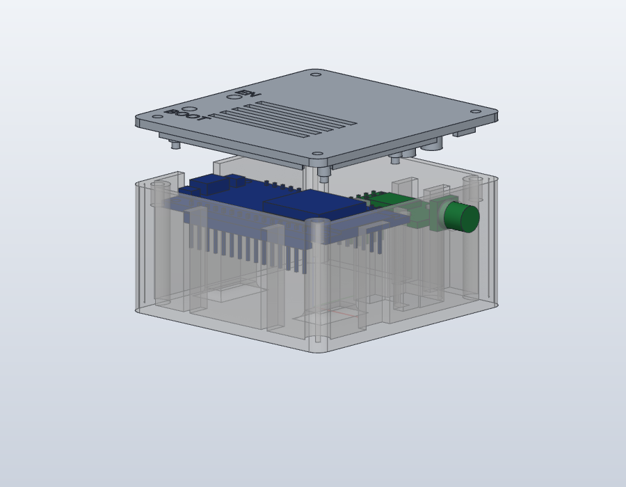
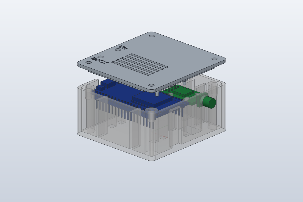
Both boards sit side by side at the same height, with all header pins pointing down into an open wiring space: 19 mm under the ESP32 headers, enough for a 14 mm Dupont plug plus room to bend the wire.
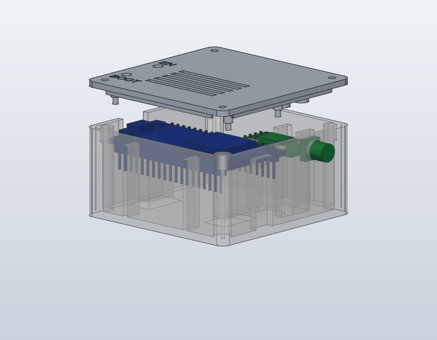
- ESP32: rests on two 5 × 12 mm support walls with filleted feet. Each of its mounting holes is only about 2.5 mm from the nearest header pin, so posts from below would collide with the jumper plugs. Instead, four stepped pegs come down from the lid: a Ø 3.2 mm shoulder that stops 0.2 mm above the board and a Ø 2.0 mm tip that goes into the hole.
- CC1101: two floor posts with Ø 2.6 mm pins go through its mounting holes, two hollow pegs on the lid fit over the pin tips and press the board down, and the SMA nut clamps it against the wall from outside.
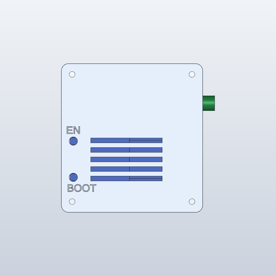
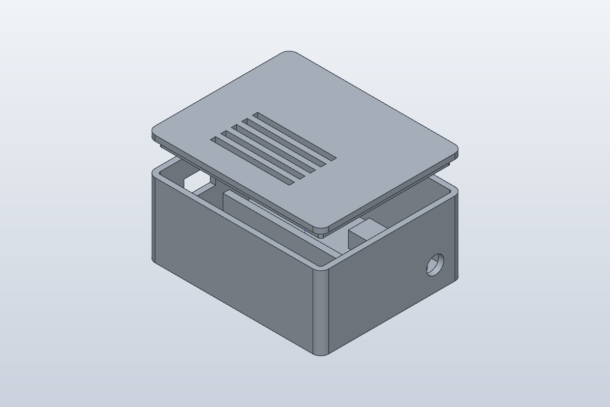
- Lid: four M2 screws into heat-set inserts, access holes for BOOT and EN with engraved labels, five vent slots, and a 7 mm gap in the lip for the SMA connector’s square housing.
| Item | Value |
|---|---|
| Outer size | Follows the board: 59.3 × 62.4 × 32 mm with the 30-pin board, 62 × 62 × 32 mm with the 38-pin board (base 30 mm, lid 2 mm), 2 mm walls |
| Lid fixing | 4 × M2 heat-set inserts (hole Ø 3.2 mm, 5 mm deep) in Ø 6 mm posts, M2 × 6 screws |
| ESP32 | 30-pin board, 51.7 × 28.4 mm, holes 46.6 × 24 mm apart, or 38-pin board, 54.4 × 28 mm, holes 50.8 × 24 mm apart |
| CC1101 | 25.6 × 15.2 mm with about 0.35 mm clearance per side |
| Wiring space | 19 mm under the ESP32 headers, about 17 mm under the CC1101 header |
| Openings | Micro-USB cut-out, Ø 7.1 mm SMA hole, BOOT and EN access holes, five vent slots |
One design, several boards
The ESP32 is described by user parameters: length, width, pins per side and the hole pattern (spacing along and across the board, distance to the USB end). A configuration table holds one row per board, so switching boards is one click. The antenna side of the box is fixed, so the CC1101 and the antenna hole never move. The USB-side wall sits 0.4 mm beyond the board’s USB end and the wall on the BOOT side 8 mm beyond the board’s edge. Walls, lid, lip, corner posts, screw holes, the USB cut-out and the ribs follow those two walls; the BOOT/EN holes, labels, lid pegs, vent slots and hold-downs follow the board.
Switching back to the 38-pin row rebuilds the earlier fixed-size design to the cubic millimetre, which confirms that the parameters reproduce it. A third board is one new row, not a redesign.
Still open: the BOOT and EN holes sit at the same distance from the USB end as on the 38-pin board. I haven’t checked yet whether the buttons on my 30-pin board are in the same place.
Printing
Print both parts without supports: the base upright, the lid plate-side down so the pegs build straight up. The Ø 2 mm peg tips are the most fragile part, so use a fine layer height. The support walls bend across their layer lines, so give them 3–4 perimeters (or 100 % infill) and print a little hotter for better layer bonding. Press the inserts in with a soldering iron at about 220–240 °C before fitting the boards. I have printed two intermediate versions; photos of the real parts will follow.
How it got there
Every request produced a new saved version, fourteen in total. Most of the changes fall into a few groups:
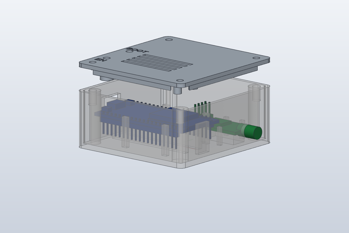
- Wiring (v5–v6). Once the pin headers were modelled, the ESP32 pins ended 3.5 mm above the floor, with no room for Dupont plugs, and the CC1101 pins pointed the other way. A redesign raised both boards and turned all pins down.
- Real dimensions (v7–v8). The first versions used typical board sizes. A phone photo showed that the CC1101 is about 4 mm shorter than assumed and that BOOT and EN were the wrong way round on the lid; the mounting pegs are based on that photo. My remark that the SMA connector sits above the board’s centre lowered the CC1101 support twice (1 mm, later another 0.7 mm).
- Size (v2, v10). M3 inserts in Ø 8 mm posts made the box grow 14 mm; switching to M2 inserts in Ø 6 mm posts won back 4 mm. The antenna hole grew to Ø 7.1 mm and the CC1101 got 0.35 mm of clearance per side.
- Strength (v11). The v9 test print broke at the free-standing 4 × 4 × 21.5 mm pillars. Volume and clash checks say nothing about strength; only the print showed it. Walls with filleted feet are about three times as stiff.
- The wrong board (v12–v14). In the printed lid the pegs were 4 mm too far apart. Calipers showed why: my ESP32 is a 30-pin board, not the 38-pin board in the photo. Instead of fixing one set of numbers, Claude turned the board into parameters, first for the pegs, then for the board model and finally for the whole box.
Measuring the boards from a phone photo
The mounting pegs started from one phone photo of the two boards on a white sheet. There was no ruler in the picture, but every board with pin headers has one built in: the pins sit on a 2.54 mm grid.
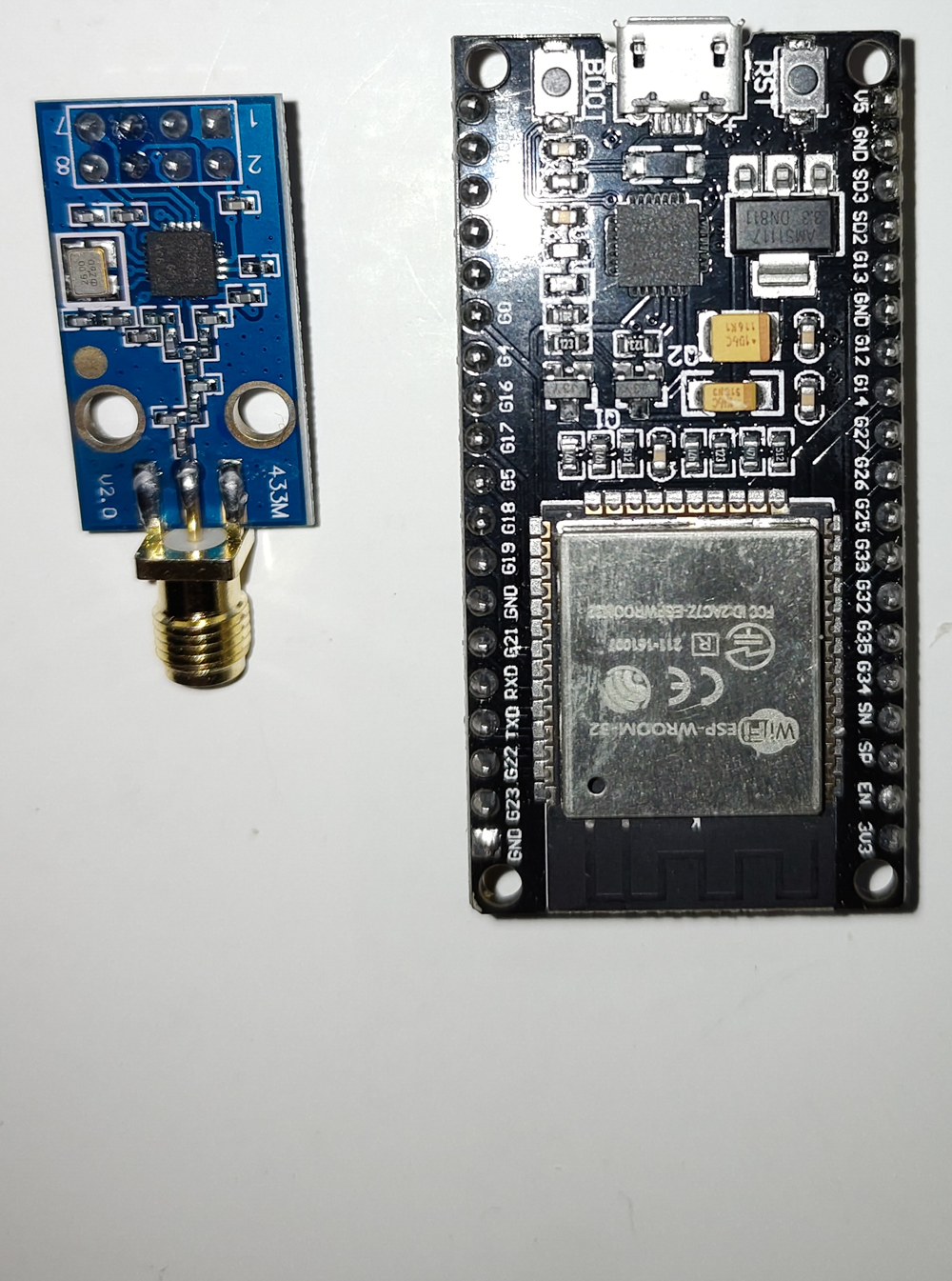
Reading positions off the downscaled image Claude had been shown gave nonsense (a 19 mm wide ESP32), and the sandbox had no Pillow or ImageMagick. So Claude used PhotoCraft, an image editor with an MCP server, to crop the original 3072 × 4096 photo and inspect the crops at full resolution. A 19-pin row spans 18 × 2.54 = 45.72 mm, which gave about 29.2 pixels per millimetre. The row spacing (25.4 mm) and the board size (54.4 × 28 mm) confirmed the scale. The ESP32’s holes form a rectangle of about 50.8 × 24 mm. The CC1101 lies at a slightly different distance from the camera, so its 2 × 4 header gave its own scale: 25.6 × 15.2 mm, holes Ø 2.8 mm, 9 mm apart and 6.8 mm from the antenna end.
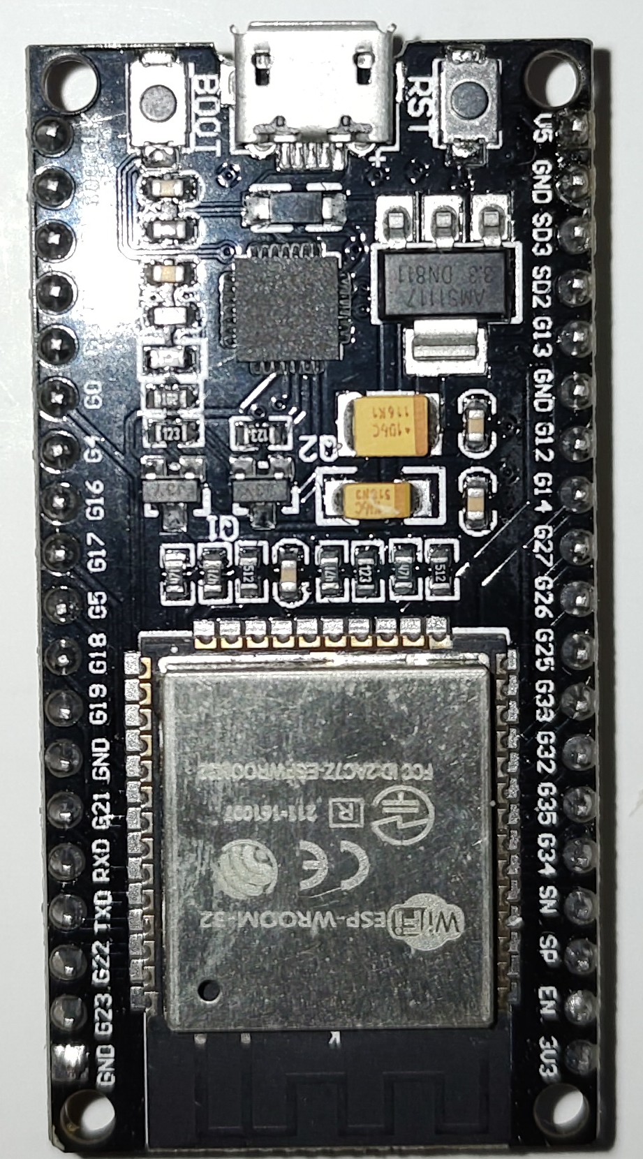
With some perspective in a handheld photo, the estimate is about ±0.3 mm, and the pins and pegs are 0.2 mm smaller than the holes. The measurement was right, but for the wrong board: the one I actually put in the box was measured with calipers and is now the 30-pin row in the configuration table.
How Claude checked its work
- Volumes calculated by hand. Before each batch of features Claude worked out the expected volume and compared it with SolidCraft’s measurement, almost always to the cubic millimetre. That matters because a cut that misses the part still reports success.
- Clash checks with the lid closed. Claude copied the lid into its closed position, ran SolidCraft’s interference check on base, lid and both boards, and deleted the copy again.
- Counting solids. After the final rewiring the lid suddenly consisted of two solids: a clamp tube had become a sealed cavity because its bore started exactly on the tube’s bottom face. Coincident faces also made SolidCraft reject three new posts earlier. Starting such features 0.1–0.5 mm deeper fixed both.
- Checking before retrying. When a large batch timed out, Claude first asked SolidCraft what was still running and measured the model. Usually the changes had been applied, and sending them again would have applied them twice; once nothing had been applied.
- Screenshots last. A render was the final check after the numbers matched.
Two more things worth knowing: PhotoCraft had copied the photo’s EXIF data, including GPS coordinates, into every crop, and Claude stripped it before anything was uploaded. And when I opened another design in the shared SolidCraft session mid-task, Claude stopped and waited for me to close it instead of reopening the enclosure over my unsaved work.
Tools used
- SolidCraft: open-source parametric 3D CAD written in Rust, with a desktop app, a browser version and an MCP server for AI agents. Website · Documentation · Source on GitHub
- PhotoCraft: open-source image editor written in Rust, part of the ArtCraft suite. Website · Source on GitHub
What I take away
As with the nest box drawings, Claude kept track of the geometry by numbers, not by looking at it, so modelling mistakes didn’t survive to the next step. But the numbers are only as good as the assumptions behind them. A photo, a test print and a pair of calipers each caught something no calculation could: wrong board sizes, pillars that snap, and a different board altogether. The answer to the last one was parameters instead of new fixed numbers, so the next board is one row in a table.